Day 1 :
Keynote Forum
Sudip Chatterjee
Regent Education and Research Foundation, India
Keynote: The study of Einstein relation in Quantum Dots Super Lattices (QDSL) of nonparabolic semiconductors: Simplified theory and suggestions for further experimental determination in biomaterials
Time : 09:30-10:00

Biography:
Sudip Chatterjee is working as an Associate Professor in the department of Basic Science at a premier Institute of India. He had received his PhD degree on some electronic transport properties of nano materials from Jadavpur University, Kolkata and he continued his research in the field of characterization and synthesis of bio-nano materials since 2002 and he had carried number of projects as the principal investigator and co-investigator under the sponsorship of some premier research institutes. He has published more than 35 papers in reputed international journals.
Abstract:
The Semiconductor Super Lattices (SLS) have found wide applications in many electronic device structures and bio devices such as photo detectors, light emitters, avalanche photo diodes, compensatory transistors, tunneling devices, genetic diodes etc. The most extensively studied SL is the one consisting of alternate layers of GaAs and Ga1-xAlxAs, owing to its fabrication. The GaAs layers form the quantum wells and the Ga1-xAlxAs layers form the potential barriers. We wish to note that, therefore mentioned SLS have been proposed with the assumption that the interfaces between the layers are sharply defined with zero thicknesses so as to be devoid of any interface effects. As the potential form changes from a well (barrier) to a barrier (well), an intermediate potential region exists for the electrons. Thus the influence of the finite thickness of the interface on the carrier dispersion law becomes very important since, the carrier energy spectrum governs all the transport properties. In this paper, we shall investigate the DMR for the most interesting case which occurs in QDSLs of graded interfaces and compare the same with that of the constituent materials by formulating the respective one dimensional electron dispersion laws. The proposed approach has been implemented and tested on an embedded system and it exhibits a good performance for monitoring/diagnosis applications.
- Nano Science and Technology | Material Science And Engineering | Nano Materials Synthesis and Characterization | Advanced Nanomaterials | Nano Medicines | Carbon Nanotechnology | Nano Electronics
Location: Paris, France
Session Introduction
Anthony N Papathanassiou
National and Kapodistrian University of Athens, Greece
Title: From local stress amplification in heterogeneous solid earth materials to hybrid ultra-piezoelectric nano-graphene polymer blends for energy harvesting
Time : 14:00-14:20

Biography:
Anthony Papathanassiou is an Assistant Professor of Experimental Solid State Physics. He got his BSc in Physics from NKUA, MSc in Condensed Matter and Materials Science from Demokritos National Centre for Scientific Research and PhD in Condensed Matter Physics from NKUA. He worked as Research Associate at various National and European projects in NKUA and Universitat Bayreuth, as research staff in NKUA and Research Scholar at Harvard University. Since 2013, as an academic member in NKUA, he is directing the Broadband Dielectric Spectroscopy and High Pressure Laboratory. His research focuses on both fundamental condensed matter physics and innovative materials science, related to non-equilibrium statistical mechanics, relaxation and phase transitions, especially, at extreme states.
Abstract:
The compression of a structurally or compositionally heterogeneous solid dictates a non-uniform internal stress field. Computer simulation on solid earth materials have proven that far-field stresses applied on different type and degree disorder earth materials yields a spatial fluctuation of the internal stress field: the stress field is locally amplified (compared to the pressure applied on the whole system). This idea inspired us to develop polymer blends Polyvinyl Acetate Polyvinyl Alcohol (PVAc) consisting of a polymer matrix hosting a fraction of piezoelectric Polyvinylidene Fluoride (PVDF) and dispersed Nano-Graphene Platelets (NGPs). Devices based on these materials are promising ones affordable, non-toxic and simply prepared energy harvesters and sensors. Hard and sharp NGPs are likely to amplify the local stress applied onto the surface of individual piezoelectric polymer grains and as a result, the effective electro-mechanical coupling of the overall material may be enhanced compared with that of neat piezoelectric PVDF. The value of the piezoelectric coefficient, which is a measure of the efficiency of a piezoelectric material to transform mechanical energy to electric one, is, in principle, a percentage of the value that neat PVDF exhibits. We present a simple strategy to augment the total effective electromechanical coupling by dispersing NGPs. Our experimental findings indicate that, by increasing the NGP mass fraction, the value of the overall piezoelectric coefficient is boosted by 150% per weight fraction of NGPs and becomes superior to values reported for neat electro-active PVdF. The synergy of the large total effective surface area available by the PVdF micro-grains and the amplification of local stresses on the piezo-active surface are by the sharp and hard NGPs dispersed in the polymer blend, is likely to optimize the electro- mechanical coupling [Figure 1].

Figure 1. The percentage difference (λ%) of the piezoelectric coefficient of a PVA-piezoactive PVDF (3:1) blends vs. the mass fraction of NGP filler, with respect to typical values reported for neat PVDF. Symbols correspond to different reference values: squares (a) β-phase circles (b) δ-phase and stars (c) β-phase. Note that, although piezoelectric PVDF constitutes merely 25 wt% of the total mass of the blend, NGPs enchances the overall piezoelectric efficiency comparable, or higher than that of neat PVDF. Inset: Open-cirquit potential difference between the two parallel surfaces of a disk shaped specimen of typical diameter 10 mm and thickness 1 mm, PVAC-PVDF (3;1) loaded with 2 wt% NGP vs. stress applied normal to the surfaces.
Wei Zhang
University College Dublin, Ireland
Title: A nanoscale shape-discovery framework supporting systematic investigations of shape-dependent biological effects
Time : 14:20-14:40

Biography:
Wei Zhang has her expertise in nanostructures synthesis and bio-nanoscale recognition and interactions. Her nanoscale shape discovery framework enables the discovery of important biological and medical outcomes in nanoscale shape biology, which can be used to connect aspects of shape to cellular readouts and then in vivo. Her work sets the milestone in this arena and defines the procedures to be followed to produce robust science from the synthesis of nanoparticles to in vivo validation. The categorization of the particle shape in the space of the PCs is an effective tool that allows going quantitatively and reproducibly from the first to the last link of this chain.
Abstract:
Nowadays it becomes inevitable for human beings to be exposed to nanostructures with distinctive complex shapes. Gain more depth knowledge regarding the nanoscale shape features regulated biological pathways becomes imperative not only for safety purposes, but also for the design of better nanocarriers for medical treatments.
One of the major barriers to figure out the link between nanoscale shape ensembles and biology is the difficulty to “identify” these irregular nano-shapes. For example, with the ever-expanding universe of nanoscale shapes, names such as “nanoflowers” and “nanostars” no longer precisely describe or characterize the distinct nature of the particles. As a basic step to eliminate the barrier we need a quantitative statistical definition of nanoscale shape that can ensure complex shape ensembles are meaningfully reproduced and their properties communicated.
Based on the above consideration, the work presented here aiming to set up a systematic framework (Figure 1) for (1) highly controlled synthesis (2) well defined identification and (3) systematically investigation of the biological effects of nanoscale shape ensembles. As shown in (Figure 2), based on a microfluidic synthesis platform we are able to achieve the tunable synthesis of nanoscale shapes and then combing traditional physiochemical characterization methods and computational shape analysis to identify each shape ensemble and finally investigate their biological impacts.
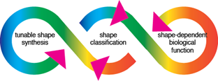
Figure 1. A nanoscale shape discovery framework.
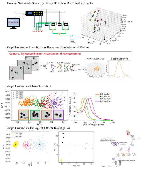
Figure 2. Detailed investigation route.
Ernst Titovets
Republican Research and Clinical Center of Neurology and Neurosurgery, Belarus
Title: Nanofluidics domain and computer simulation of water metabolism in the brain cortex
Time : 16:00-16:20

Biography:
Ernst Titovets, M.D., PhD is a researcher, author, translator and interpreter was born in Krasnoyarsk, Siberia. He graduated from the Minsk State Medical Institute and undertook post-graduate research in biochemistry. He earned his PhD degree from the Academy of Sciences of Belarus for his research on endergonic transport of Ca++ by the mitochondria. His Doctor of Sciences Degree in biology he obtained from the St. Petersburg State University, Russia for his pioneering research on the biochemical action mechanism of new aminodervatives of orthobenzoquinone. Appointed to a number of scientific research councils, he has authored or co-authored four research books, 14 patents and over 400 research papers and as an interpreter, he translated three books. As an Author, he wrote a book Oswald: Russian Episode that has appeared in three editions in the USA. The book presents an in deep historic investigation of life of Lee Harvey Oswald, an alleged assassin of the President John Kennedy. Currently he is concentrated on a research on brain water metabolism and related issues conducted from the nanofluidic approach. He is a principal researcher, at the Republican Research and Clinical Centre of Neurology and Neurosurgery in Minsk, Belarus where he heads a scientific research group.
Abstract:
Brain water metabolism is involved in cell communication, transfer of signaling molecules, neurotransmitters, energy substrates and gases, heat exchange, etc. A number of pathologies including Alzheimer’s disease, idiopathic normal pressure hydrocephalus, migraine, traumatic brain injury and stroke, brain edema, etc. directly or indirectly arise from disorders in brain water metabolism.
There are the two mutually excluding basic views at present on brain water metabolism. A conventional theory maintains that the brain nanodimentional extracellular space presents a diffusion barrier to water movement. A new theory, based on an interdisciplinary approach and adopted here, makes it possible to treat the brain extracellular space as a nanofluidic domain where water flow is governed by the slip-flow mechanism. Contrary to the diffusion-barrier theory, the new one suggests fast water movement in the extracellular space.
Computer simulations of brain water metabolism have been carried out using a cuboid nanofluidic model. The model encompasses layers I-IIIb of the brain cortex and incorporates a central draining venule surrounded by four penetrating arterioles with the intervening capillary network. Aquaporin AQP4 presents a rate-limiting stage in the overall water transfer across the blood-brain barrier, i.e. between the blood and the brain parenchyma. The extracellular space is viewed as a nanofluidic domain. Computer simulations have produced a detailed 3D topography of brain water metabolism in terms of the volumetric water fluxes. Physiological and pathophysiological significance of the obtained results is discussed.
Jufan Zhang
University College Dublin, Ireland
Title: Manufacturing of large area solid-state nanopore array
Time : 16:20-16:40

Biography:
Jufan Zhang, Assistant Professor and Lecturer in School of Mechanical and Materials Engineering, Principal Investigator in Centre of Micro/Nano Manufacturing Technology, University College Dublin, Ireland. He leads the research in manufacturing of solid state nanopore array and corresponding biomedical applications by collaborating with academic and industrial partners. He has chaired 10+ researches funding and made 50+ peer-reviewed publications and 7 patents on nanomanufacturing, ultra-precision machining, biomedical devices and optics. He has given over 10 keynote/invited talks in the recent one year on nanomanufacturing and biomedical research. He is the Member of Irish Manufacturing Council, Member of International Academy of Engineering and Technology, Member of International Society for Nanomanufacturing. He is the Chair of Organizing Committee of the 8th International Conference on Nanomanufacturing and the 4th AET Symposium on ACSM and Digital Manufacturing
Abstract:
Nanopore brings extraordinary properties for a variety of potential applications in various industrial sectors. Since manufacturing of solid-state nanopore was firstly reported in 2001, solid-state nanopore has become a hot topic in the recent years. An increasing number of manufacturing methods have been reported, with continuously decreased sizes from hundreds of nanometres at the beginning to approximate one nanometre until recently. To enable more robust, sensitive and reliable devices required by the industry, researchers have started to explore the possible methods to manufacture nanopore array which presents unprecedented challenges on the fabrication efficiency, accuracy and repeatability, applicable materials and cost. As a result, the exploration of fabrication of nanopore array is still in the fledging period with various bottlenecks. This presentation introduces an efficient and cost-effective manufacturing process chain for fabricating large area solid state nanopore array. The authors successfully fabricated the 20 nm nanopore array in a 15 mm×15 mm area, with relatively uniform pore shape and size. The experiments also indicated a possible way to reduce the pore size down to 1 nm simultaneously modify the geometry of nanopore channel, which would be a breakthrough to facilitate the high-resolution DNA sequencing. Some representative applications of nanopore array include DNA/RNA sequencing, energy conversion and storage, water desalination, nano-sensors, nanoreactors and dialysis [Figure 1].
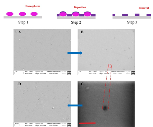
Figure 1. The nanopore array fabricated by the hybrid method. Top: the schematic flow plot of process chain. A. Nanospheres around 20 nm in diameter distribute on the substrate, then with 4 nm Pt film deposited; B. SEM images after ultrasound for 5 min; C. SEM images of one nanopore zoom-in (magnified 500 K; scale bar: 300 nm); D. SEM image of nanopores after ultrasound for 15 min.
Jun Gou
University of Electronic Science and Technology of China, China
Title: Surface-illuminated ultra-fast Si and PbSe infrared detectors with enhanced efficiency via periodic microstructures
Time : 16:40-17:00

Biography:
Gou studied Optical Engineering at University of Electronic Science and Technology of China (UESTC) and graduated as MS in 2010. He received his PhD degree in 2014 at the same institution. Now he works at School of Optoelectronic Science and Engineering, UESTC. He is dedicated to the research of uncooled infrared and terahertz detectors. In recent years, he has published more than 30 research articles in SCI(E) journals, co-authored 1 English monograph and won the first prize of Science and Technology Progress of Sichuan Province and more than 20 national invention patents.
Abstract:
CMOS-process-compatible silicon (Si) based detectors could lead to a cheaper and better integrated fibre-optic communication system. However, traditional Si photodiodes with a weak absorption coefficient of Si can hardly achieve a high External Quantum Efficiency (EQE) and a high data transmission rate simultaneously at near-infrared wavelengths used for data communication. In this work, in order to increase the EQE of Si based MSM photodiodes while maintaining a high-speed operation, periodic arrays of cylindrical-shaped photon-trapping holes are integrated in thin absorption regions between metal fingers. The holes are arranged in square and hexagonal lattices with different designs of hole diameter, depth and period. Theoretical and experimental study reveals that a beam of vertically incident light is guided laterally and confined in the nanostructured Si film. Si based MSM photodiodes with integrated photon-trapping hole structures has an enhanced EQE of 61% and an ultra-fast impulse response (full-width at half-maximum) of 25 ps. PbSe film is prepared on Si by an evaporation process to realize broadband high efficiency up to 1550 nm. By integrating photon-trapping holes, the absorption and EQE of PbSe based MSM photodiodes are also significantly improved. The detector with microstructured holes exhibits over 500% enhancement of EQE compared to the device without hole structures.