


Jufan Zhang
University College Dublin, Ireland
Title: Manufacturing of large area solid-state nanopore array
Biography
Biography: Jufan Zhang
Abstract
Nanopore brings extraordinary properties for a variety of potential applications in various industrial sectors. Since manufacturing of solid-state nanopore was firstly reported in 2001, solid-state nanopore has become a hot topic in the recent years. An increasing number of manufacturing methods have been reported, with continuously decreased sizes from hundreds of nanometres at the beginning to approximate one nanometre until recently. To enable more robust, sensitive and reliable devices required by the industry, researchers have started to explore the possible methods to manufacture nanopore array which presents unprecedented challenges on the fabrication efficiency, accuracy and repeatability, applicable materials and cost. As a result, the exploration of fabrication of nanopore array is still in the fledging period with various bottlenecks. This presentation introduces an efficient and cost-effective manufacturing process chain for fabricating large area solid state nanopore array. The authors successfully fabricated the 20 nm nanopore array in a 15 mm×15 mm area, with relatively uniform pore shape and size. The experiments also indicated a possible way to reduce the pore size down to 1 nm simultaneously modify the geometry of nanopore channel, which would be a breakthrough to facilitate the high-resolution DNA sequencing. Some representative applications of nanopore array include DNA/RNA sequencing, energy conversion and storage, water desalination, nano-sensors, nanoreactors and dialysis [Figure 1].
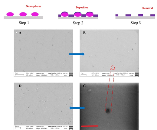
Figure 1. The nanopore array fabricated by the hybrid method. Top: the schematic flow plot of process chain. A. Nanospheres around 20 nm in diameter distribute on the substrate, then with 4 nm Pt film deposited; B. SEM images after ultrasound for 5 min; C. SEM images of one nanopore zoom-in (magnified 500 K; scale bar: 300 nm); D. SEM image of nanopores after ultrasound for 15 min.